當(dāng)前位置:首頁(yè) > 產(chǎn)品中心 > 二維材料 > 六方氮化硼 > 六方氮化硼晶體(20片裝)


簡(jiǎn)要描述:六方氮化硼晶體(20片裝) hBN(Hexagonal Boron Nitride)-Crystal晶體尺寸:~1mm電學(xué)性能:絕緣體/半導(dǎo)體晶體結(jié)構(gòu):六邊形晶胞參數(shù):a = b = 0.2502 nm, c = 0.6617 nm, α = β = 90°, γ = 120°晶體類型:合成晶體純度:*
 產(chǎn)品型號(hào):
  廠商性質(zhì):生產(chǎn)廠家
 更新時(shí)間:2024-06-03
 訪 問 量:1479
相關(guān)文章
Related Articles詳細(xì)介紹
六方氮化硼晶體(20片裝) hBN(Hexagonal Boron Nitride)-Crystal
晶體尺寸:~1mm
電學(xué)性能:絕緣體/半導(dǎo)體
晶體結(jié)構(gòu):六邊形
晶胞參數(shù):a = b = 0.2502 nm, c = 0.6617 nm, α = β = 90°, γ = 120°
晶體類型:合成
晶體純度:*

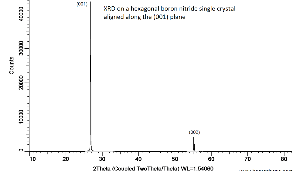
X-ray diffraction on a hexagonal boron nitride single crystal aligned along the (001) plane. XRD was performed at room temperature using a D8 Venture Bruker. The 4 XRD peaks correspond, from left to right, to (00l) with l = 1, 2, 3

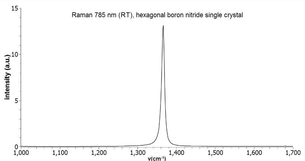
Raman spectrum of a single crystal hexagonal boron nitride (h-BN). Measurement was performed with a 785nm Raman system at room temperature.

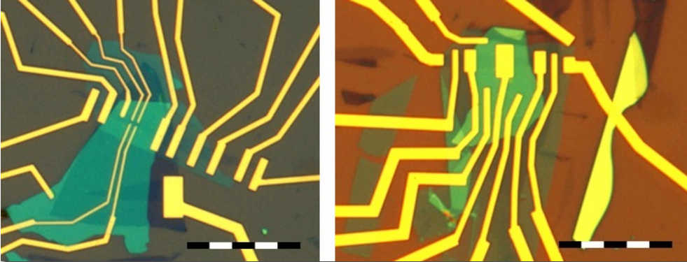
Device at left side: Fabrication of a high mobiltity bilayer graphene. This field effect transistor is fabricated using the polymer 2D_CL_PC ( click here ). The device is composed out of four 2D layers. The bilayer graphene is encapsulated between two hexagonal boron nitride crystals (h-BN). The fourth layer is a thin layer of graphite (HOPG) which is used as a backgate. Scale bar is 20μm. Device at right side: This device is similar to the one at the left side, here we added on the top hexagonal boron nitride layer a gold electrode in order to apply a top gate voltage to the hBN encapsulated bilayer graphene. Scale bar is 20μm
產(chǎn)品咨詢
聯(lián)系我們
上海巨納科技有限公司 公司地址:上海市虹口區(qū)寶山路778號(hào)海倫國(guó)際大廈5樓 技術(shù)支持:化工儀器網(wǎng)掃一掃 更多精彩

微信二維碼

網(wǎng)站二維碼